
Quantum bits (qubits) form the foundation of every quantum computer, carrying out complex calculations that classical computers are not always capable of.
If we can scale quantum computers to the point where they can carry out trillions of quantum operations (Quops), then they hold tremendous promise with an estimated $1.3 trillion in value by 2035 across multiple industries. They will also become integral part of next-generation Exascale High Performance Computing (HPC) including the on-premises compute resources used by governments and businesses worldwide.
We’re not there yet. Today’s quantum computers are capable of a few hundred Quops, which is roughly 10 orders of magnitude less than required to do something ‘useful’ with these machines.
This is because qubits are by nature highly error prone. So, we must correct these errors to scale quantum computers and unlock their true value to society.
This is where quantum error correction comes in. This is a set of techniques used to protect the information stored in qubits from errors and decoherence caused by noise. To achieve quantum error correction at scale (and with the required levels of accuracy, speed and resource efficiency) is a monumental engineering challenge.
At Riverlane, our core focus is quantum error correction. Our Quantum Error Correction Stack (Deltaflow) is roughly comprised of two components: Deltaflow.Control and Deltaflow.Decode. Deltaflow.Control “reads” and “writes” the qubits, similar to the read and write functions in a classical computer to maintain the qubits’ delicate quantum states.
Deltaflow.Decode ensures the quality and reliability of the qubits, preventing them from becoming just noise. You can think of them together as a Solid-State Disk controller: one part reads and writes the memory cells; another identifies and corrects any errors encountered.
In this article, the focus is on the Deltaflow.Control system and we look at some of the innovations that will give us more responsive and better performing quantum systems.
Minimising configuration deadtime
Qubits must be controlled and manipulated using control and measurement signals to run their complex calculations. These signals are highly synchronised, precisely shaped Radio Frequency (RF) pulses used to directly or indirectly (i.e. via optical modulation) drive the qubits. They are largely produced using a combination of off-the-shelf and custom hardware, with FPGAs being an integral part of most systems.
The electronic systems behind these control and measurement signals serve as a bridge between quantum programming language and quantum information processors.
In a typical setup, users write code - referred as quantum circuits - on their laptop or on a HPC node, the code then gets compiled and transmitted (over a local network or over the cloud) to a second CPU that handles the configuration of one or more FPGAs. A rule of thumb: the more the qubits, the more the FPGAs that are required to control them.
Because the circuitry inside an FPGA processor is not hard etched, then the FPGA processor can be programmed and updated as needed to best meet the needs of the Control system.
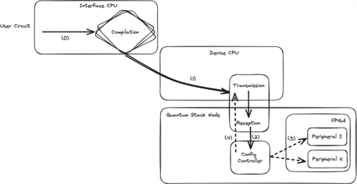
Figure 1: Standard quantum stack implementation
In a super-dynamic quantum ecosystem, this flexibility is key and alternative electronics are not an option. ASIC solutions are still cost-prohibitive (volumes are too small) and CPUs are not equipped with the necessary components to do the job.
A quantum circuit could take anything from a few microseconds to hundreds of milliseconds to run, depending on the qubit type and on the complexity of the calculation (jargon: circuit depth) and other factors.
If we can reduce deadtime between quantum routines (e.g. by reducing their configuration time), then the efficiency of our quantum computers increases. We achieve more runs per day and that means research can move faster as the time between developing and testing an idea shortens.
What’s the innovation?
If we look at Figure 1, the device CPU needs to propagate (part of) the configuration to multiple FPGAs, wait for the internal configuration to complete and finally start the quantum routine when all FPGAs are configured by sending some form of start command.
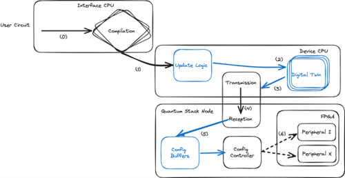
Figure 2: Optimised stack for high throughput execution
The first bottleneck occurs when we configure multiple FPGAs. Configuration entails setting various internal memories, normally using high-throughput internal connections (up to 4GB/s or 8 times as fast as a standard SSD) in a sequential way. Even setting 4KB of memories requires 2μs (more specifically 500 clock cycles at 250Mhz).
Our second bottleneck occurs when we buffer the configuration on the FPGA. Transmitting the same 4KB over an ultra-low-latency link will result in approximately 1μs of deadtime.
Even if we used highly optimised network interfaces, this still brings us to a total of 3μs of deadtime.
But there’s one last bottleneck to consider: when the configuration is complete a “job done” signal must go back to the device CPU. This will require transmitting back a small ACK (message sent to indicate whether the data packet was received), adding approximately 100ns to the deadtime. So, we now have a total of 3.1μs.
The solution? Leverage a digital twin of the system to reduce the transmissions overhead (send only what changes) and drop the ACK phase (everything is hardware synchronised). In practice, build a fully streaming interface for configurations.
Be smart
The interface that connects the QPU and the classical electronics can be extremely bandwidth limited (small number of wires, limited power budgets) and an unwanted source of noise. Every technique that leads to noise reduction allows for more/faster electronics to operate in the quantum control system, with no increase in the total dissipated energy. This leads to more capable quantum stacks, that can control more qubits, correct more errors, or a combination of the two.
Our solution look to minimises noise over the transmission wires where the digital control signals are compressed at the classical interface.
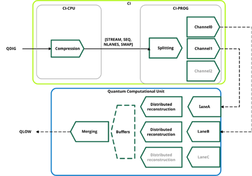
Figure 3: Diagram from our earlier patent, which covers a method for transmitting control signals from a classical computing interface to a QPU
Compression techniques exploit redundant information in the data to generate a representation that requires less data to be transmitted. The less data we send, the less bandwidth we use, and the less power we consume.
To understand the benefits that compression brings, and the importance of doing it in an energy efficient way, we need to understand the full data chain.
In a quantum computing stack, as quantum circuits get converted to low-level signals, the associated amount of data grows. Whilst one quantum gate can be stored in a few bytes (e.g. in OpenQASM2.0 then a Hadamard gate becomes the string: “h q[0];”), the associated low-level signals might easily take kilobytes or more.
Unfortunately, moving data requires energy and the more energy that is used to move data then the less is available to control the qubits. As shown in Figure 2, this might happen in the parts of the quantum stack where we want to dissipate as little energy as possible.
For example, the dilution fridges used by silicon/superconducting qubits are constructed in stages, with the colder stages less capable of dissipating heat. By compressing the data before transmitting and decompressing it afterwards, we could reduce the noise radiated in the system and reduce the generated heat.
Potentially, however, the compression/decompression process could introduce noise and, therefore, finding the right balance between the heat generating by compressing vs transmitting data is key.
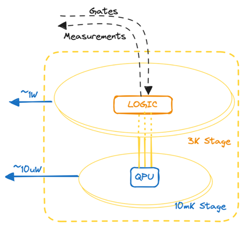
Figure 4: Physical limitations impose extremely challenging power budgets as we get closer to the qubits (QPU).
A universal solution might not be possible. We might be in a scenario in which we are power bound at the transmitter side (e.g. transfer information out a colder cryogenic stage), at the received side (e.g. send low-level control information into a colder cryogenic stage) or on both (transfer information within components in the cryogenic system), for example.
Each of these systems will likely need a bespoke solution. Our invention can guide this process by first identifying the optimal compression/decompression scheme in four steps:
- Load the expected data patterns into our engine. One way to generate the data pattern is to set the distribution of quantum instructions to be executed and then map the signals that need transmission.
- Consider the input properties of the digital logic used in the system and the power budgets. A non-exhaustive list might include the number of transmission wires, memory active and passive consumption, flip-flop toggle energy, clocking tree energy dissipation. Table 1 uses open-source data to elaborate on this concept.
- Set the power budgets for compression and decompression phases.
- Get the result. Multiple compression/decompression schemes are analysed, and their power budgets estimated and presented to the user.
Secondly, the transmission per-se is analysed and the lowest noise transmission scheme is identified by leveraging information such as transmission protocol(s) used, wire emission and extrapolated crosstalk. All the transmission lanes are driven independently to maximise the flexibility of the solution.
This invention leapfrogs the design phase by tackling one of the hardest-problems in quantum control in a no-code fashion.
While there are many engineering challenges to address to unlock useful quantum computing – quantum error correction is the key to achieving this.
Author details: Marco Ghibaudi is VP Engineering at quantum error correction company Riverlane


