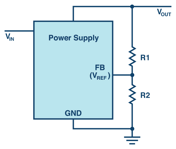
This is accomplished in most integrated power supply circuits, as well as switching and linear regulator ICs, with the help of voltage dividers. The ratio of the two resistance values must be suitable to enable the desired output voltage to be set.
Figure 1 shows a voltage divider. The internal reference voltage (VREF) and the desired output voltage determine the ratio of the resistance values, as seen in Equation 1:

The reference voltage VREF is defined by the switching regulator or linear regular IC, and is usually 1.2V, 0.8V, or even 0.6V. This voltage represents the lowest voltage that the output voltage (VOUT) can be set to. With the reference voltage and output voltage known, there are still two unknowns in the equation: R1 and R2. One of the two resistance values can now be selected relatively freely, as usual values lie below 100kΩ.
If the resistance values are too low, the power loss due to the constantly flowing current VOUT/(R1 + R2) during operation is extremely high. If R1 and R2 each had a value of 1kΩ, then a continuous leakage current of 1.2mA would flow at an output voltage of 2.4V. This corresponds to a power loss of 2.88mW generated by the voltage divider alone.
Depending on how precisely the output voltage should be set and how high the current in the power supply error amplifier at the FB pin is, Equation 1 can be specified more precisely through consideration of this current.

Figure 1. Voltage divider in a voltage regulator for adjustment of output voltage.
However, the resistance values should not be too high. If the resistance values were each 1MΩ, we would only have a power loss of 2.88µW. A major disadvantage of this resistor dimensioning with very high values is the fact that it results in a very high feedback node impedance. The current flowing into the feedback node can be very low depending on the voltage regulator.
As a result, noise can couple to the feedback node and directly affect the control loop of the power supply. This can stop the regulation of the output voltage and lead to control loop instability. Especially in switching regulators, this behaviour is critical, because noise arises due to the rapid switching of currents and can couple to the feedback node.
Useful resistance values for R1 + R2 lie between 50kΩ and 500kΩ depending on the noise expected from other circuit segments, the value of the output voltage, and the need to reduce the power loss.

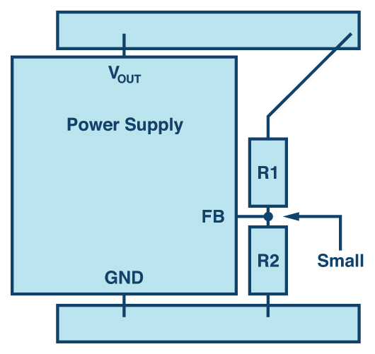
Figure 2. Example of a well-placed voltage divider in a power supply.
Another important aspect is the placement of the voltage divider on the board layout. The feedback node should be designed to be as small as possible so that very little noise can couple to this high impedance node. Resistors R1 and R2 should also lie very close to the feedback pin of the power supply IC. The connection between R1 and the load is usually not a high impedance node and can hence be designed to have a longer trace. Figure 2 shows an example of resistors placed close to the feedback node.

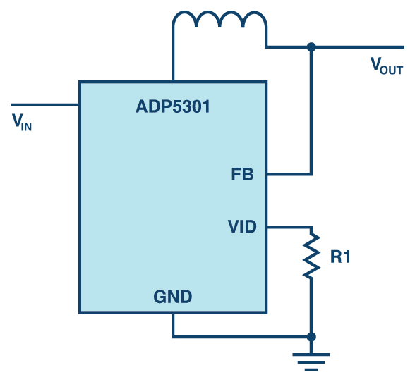
Figure 3. Adjustment of the output voltage without a continuous power loss in the voltage divider.
To reduce the power loss of a voltage divider, especially in ultra-low power applications such as energy harvesting, some ICs, like the ADP5301 step-down regulator, feature an output voltage setting function in which the value of a variable resistor at the VID pin is only checked once during start-up. This value is then stored for ongoing operation without current constantly flowing through a voltage divider. A very sensible solution for highly efficient applications.
Author details: Frederik Dostal, Field Applications Engineer, Analog Devices
To contact the author use the following link:
To read further Design Tips from ADI follow the link below.


