
With projections estimating a global market opportunity of around $4.3 billion by the end of the decade, this technology is gaining traction in the electronics industry.
Here Nir Sade, General Manager AME at Nano Dimension, explores how AME is reshaping product development and production, paving the way for a future where electronics manufacturing is more agile, efficient, and decentralised.
Could you begin by introducing Nano Dimension, and explaining what it is you do?
Nano Dimension offers a variety of Digital Manufacturing technologies serving customers across vertical target markets such as aerospace and defence, advanced automotive, high-tech industrial, speciality medical technology, and R&D and academia.
With its suite of digital manufacturing technologies, Nano Dimension is enabling prototyping and high-mix-low-volume production, along with IP security, design-for-manufacturing capabilities, and more sustainable means of fabrication.
As part of the Digital Manufacturing offering, Nano Dimension is a leading provider of additively manufactured electronics (AME) technology, manufacturing 3D printers that provide an innovative in-house method of designing, developing and manufacturing high-value PCBs and electronic devices.
Our holistic solution, encompassing hardware, software, material and process, is largely used by customers in R&D, spanning aerospace and defence, medical, industrial products, and scientific research. We focus on delivering industrial grade solutions, working closely with our customers to enable this.
What makes AME so compelling to the electronics industry, and what challenges does it address and overcome?
The appeal of AME comes down to four main factors. Firstly, this technology is revolutionising R&D efforts in the electronics industry, as it provides greater freedom of design through geometry enabling the creation of smarter and smaller products with integrated non-planer electronics. Today’s technology allows designers to simultaneously 3D print conductive and dielectric material to produce completely new designs, including integrated printed components, such as twisted coils, capacitors, and any angle connection of conductors. These capabilities simplify the assembly steps and improve signal integrity.
Closely related to this is the ability to rapidly prototype parts in-house, particularly for complex small devices such as antennas, sensors and connectors. Traditional prototyping methods can be costly and time consuming to produce small batches, making iterative design difficult, whereas AME simplifies this process and enables agile hardware development.
Third, AME enables the reshoring of production and the use of digital inventories for on-demand, on-site creation of electronics spare parts. This is highly beneficial, particularly in cases where unexpected geo-political or other disruptions affect traditional supply chains. Additionally, this approach reduces reliance on China.
Last but certainly not least, AME offers the ability to rapidly 3D print cost-effective, multi-layer prototype PCBs. Traditional PCB prototyping involves sending the design to PCB manufacturers, but producing them in-house with AME streamlines product development, shortening lead times, eliminating dependency on external vendors, and allows the simultaneous printing of multiple designs simultaneously. This results in faster functional prototyping than any other method, ultimately accelerating time to market.
Would it be fair to say that AME offers similar prototyping benefits to standard 3D printing, which has already been widely adopted in other industries?
That’s a reasonable comparison. The key distinction is that AME is still at a relatively early stage of industry adoption. While it offers huge advantages, such as simplifying and accelerating prototyping, design engineers are accustomed to traditional methods. As with any other new technology, it takes time for design engineers to fully grasp, appreciate and ultimately transition away from familiar workflows. AME is at a similar stage today as mechanical’ 3D printing or AM was a few years ago. Just as 3D printing has become the go-to for designers – who are now reaping the benefits of reduced labour, simplified processes, and cost efficiencies – I’m confident adoption of AME among electronics industry designers will continue to accelerate.
How is Nano Dimension working to educate the industry and encourage wider adoption of AME?
A key challenge with AME is that there isn’t yet an established knowledge base for designing 3D printed electronics. To bridge this gap, we are actively collaborating with numerous universities and research institutes to explore real-world applications. For example, together with the University of Stuttgart and the BMBF Cluster4Future QSens, we are leveraging our multi-layer, multi-material DragonFly IV 3D printer to accelerate advancements in quantum devices.
To instil trust in the AME offering, we are working with IPC, the global organisation for electronics manufacturing, to develop IPC Standard 2581 – a dedicated standard for the qualification and production of 3D printed electronics. To support this effort, we have contributed our internal procedures and provided a recognised industry expert to lead the AME sub-committee and specific task groups.
Establishing trust in AME is crucial, so we aim to develop an industry-wide qualification and acceptability standard, along with test methods and design guidelines based on reliability requirements that are globally accepted by consumers of AME products. Crucially, for manufacturers and OEMs, this will ensure that AME can be produced consistently and dependably, regardless of the manufacturing location.
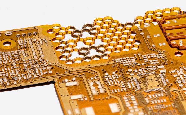
Above: 3D printed AME enables the creation of more advanced products.
What future applications of AME do you foresee, and when might we expect to see them in real-world use?
We expect breakthrough developments in the way AME is used soon, as customers we’re working with have already qualified the first applications to be manufactured using the benefits of AME. For example, a defence organization developed and qualified an antenna for air-borne devices. This case demonstrates the unique advantages 3D design freedom and the advancements in materials and production processes, that met the customers’ requirements, as well as the advantages of AME over traditional manufacturing – simplifying production and reducing steps.
We see a similar trend towards low volume manufacturing of high value applications, such as sensors and connectors that require miniaturization, lightweighting, flex and rigid-flex materials, and will therefore benefit from AME.
Do you have any final predictions for the future of AME?
For Nano Dimension and other manufacturers in the industry, developments in materials, software, and processes will continue to be critical. Although we’re still educating the market, much like the pioneers of mechanical 3D printing around 30 years ago, the trend is clear. We foresee increasing adoption of AME for high-value applications, starting with defence and aerospace segments and then moving towards other industrial sectors.


