
As technology advances, PCBs themselves are becoming more complex, requiring intricate designs and precise development execution. These complexities, combined with the need for rapid development cycles, necessitate a collaborative approach, bringing together various experts and stakeholders to ensure the creation of efficient, reliable, and innovative electronic products.
Effective collaboration among team members and across different disciplines and domains can significantly enhance innovation, reduce errors, and improve overall efficiency. In this article, we’ll explore the importance and benefits of collaboration as well as strategies for fostering it in PCB design.
Collaboration in PCB design is crucial for many reasons:
Complexity Management — Modern PCBs are highly complex, often featuring multiple layers, intricate routing, and a variety of components. Collaboration ensures that different aspects of the design, such as electrical, mechanical, and thermal considerations, are seamlessly integrated.
Enhanced Innovation and Creativity — Collaboration fosters an environment where diverse ideas and creativity can flourish. Team members can brainstorm, share ideas, and build on each other’s suggestions, leading to innovative solutions and more effective designs. When engineers, designers, and other stakeholders work together, they bring unique perspectives and expertise to the table. This diversity can lead to innovative solutions that might not emerge in a siloed environment. For example, a mechanical engineer/designer might suggest an innovative way to arrange components to improve thermal management, while an electrical engineer/designer can optimize the circuit layout for better performance. Such cross-disciplinary, bi-directional interactions are crucial for pushing the boundaries of PCB design.
Error Reduction — Collaborative design helps in early identification and correction of errors. Cross-functional teams can provide diverse perspectives, leading to more thorough design reviews and validation processes.
Improved Design Accuracy and Quality — PCB design involves meticulous attention to detail to ensure that the final product functions correctly. Collaboration among team members helps in catching errors early in the design process. Peer reviews, for instance, allow team members to scrutinize each other’s work, identifying potential issues that might have been overlooked. This collaborative vetting process significantly enhances the overall quality and accuracy of the PCB design.
Speed, Efficiency, and Problem Solving — Collaboration accelerates the design process. By working together, teams can parallelize tasks, quickly resolve issues, and share knowledge, reducing the time from concept to production. Problems in PCB design can be complex and multifaceted, requiring input from various experts to resolve. When team members collaborate, they can quickly pool their knowledge to troubleshoot issues effectively. This collective problem-solving approach not only speeds up the resolution process but also leads to more robust solutions. For example, if there is an issue with signal integrity, input from both the layout designer and the signal integrity engineer can be critical in identifying and addressing the root cause.
Streamlined Workflow and Reduced Time-to-Market — Collaborative efforts streamline the PCB design workflow, reducing redundancies and improving communication. By working together, team members can synchronize their tasks, ensuring that each phase of the design process progresses smoothly. This coordination is vital for meeting tight deadlines and reducing time-to-market. Tools that support collaborative design, such as cloud-based PCB design software, further enhance this streamlined workflow by allowing real-time collaboration and updates.
Enhanced Knowledge Sharing and Skill Development — Collaboration in PCB design is also a valuable opportunity for knowledge sharing, mentorship, and skill development. Junior engineers and designers can learn from their more experienced colleagues, gaining insights into best practices and advanced techniques. This knowledge transfer is beneficial not only for the individuals involved but also for the organization, as it helps build a more skilled and versatile team.
Greater Flexibility and Adaptability — The rapidly evolving nature of technology demands flexibility and adaptability in PCB design. Collaborative teams are better equipped to handle changes in project requirements or unexpected challenges. With a collaborative approach, team members can quickly realign their efforts and make necessary adjustments to the design, ensuring that the project stays on track despite any disruptions.
Increased Accountability and Ownership — When team members collaborate, there is a heightened sense of accountability and ownership of the project. Each member understands their role and how their contributions impact the overall success of the design. This sense of responsibility fosters a more committed and motivated team, leading to higher quality outcomes and a greater likelihood of project success.
The benefits of effective collaboration in PCB design are significant in many aspects. Improved design quality by collaborative efforts results in more robust and optimized designs. Shared expertise and collective problem-solving lead to higher-quality outcomes. By streamlining the design process and minimizing iterations, collaboration brings products to market faster. This is crucial in the highly competitive electronics industry. Cost efficiency through early error detection and resolution reduces the need for costly redesigns and re-work. Efficient resource utilization and parallel task execution also contribute to cost savings. Lastly, one of the most crucial benefits of collaboration pertains to communication.
For years, the industry phrase, “Communication…Communication…Communication!” has continued to be amplified and stressed when it comes to industry best practices in successful PCB design. You cannot have too much communication during a project design cycle. Enhanced documentation and communication between all stake holders (both internal and external) regarding multidomain and multidiscipline integrations and collaboration ensures that all team members and stakeholders are on the same page and the design intent is clearly conveyed to manufacturing.

To foster effective collaboration in PCB design, organizations can adopt several strategies:
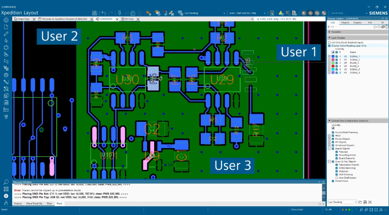
Utilize Collaborative Software Tools — Modern PCB design tools like Siemens Xpedition and PADS Professional, Cadence Allegro and OrCAD, Altium Designer, and Zuken, just to name a few, offer collaborative features, including version control, real-time commenting, and shared workspaces. These tools enable multiple designers to work on the same project simultaneously.
Implement Version Control Systems (VSCs) — Version control systems allow teams to track changes, manage revisions, and collaborate more effectively. They ensure that everyone is working with the latest design files and can easily revert to previous versions if needed.
Encourage Cross-Functional Teams — Bringing together engineers from different disciplines—such as electrical, mechanical, and software engineering—ensures that all aspects of the design are considered. Cross-functional teams can identify potential issues early and propose comprehensive solutions.
Conduct Regular Design Reviews — Scheduled design reviews involving all stakeholders help in early detection of potential problems. These reviews provide a platform for feedback, ensuring that the design meets all requirements and standards.
Leverage Cloud-Based Platforms — Cloud-based design platforms facilitate remote collaboration, enabling team members to work together regardless of their physical location. These platforms offer centralized data storage, easy access to design files, and seamless integration with other tools.
Foster a Collaborative Culture — Creating a culture that values teamwork, open communication, and mutual respect is essential for successful collaboration. Encouraging team members to share ideas and provide constructive feedback enhances the overall design process.
Collaboration is indispensable in PCB design, bringing numerous advantages that enhance the innovation, quality, and efficiency of the design process. Embracing collaboration transforms the PCB design process from a solitary endeavour to a synergistic journey toward creating cutting-edge electronic products. Collaboration is not just a trend but a necessity in today’s fast-paced and complex electronics industry.
By leveraging collaborative tools, fostering cross-functional teamwork, and encouraging a culture of open communication, organizations can significantly improve their PCB design processes, take advantage of the diverse expertise of team members, streamline workflows, and accelerate the development of cutting-edge electronic products. The result is higher-quality designs, reduced time-to-market, and cost savings, ultimately leading to greater innovation and competitiveness in the market. As technology continues to evolve, the importance of collaboration in PCB design will only grow, making it a fundamental aspect of successful electronic product development.
Author details: Stephen V. Chavez, Principal Technical Product Marketing Manager – Siemens EDA, and Chairman – PCEA
This article was sponsored by Siemens Digital Industries Software


