
While the dot com crash caused the industry some problems, photonics has continued to find wider application, although telecommunications remains a major end user.
As photonics finds wider application, the demands on its performance grow. While some researchers are looking towards silicon photonics as a means of improving performance, others believe that graphene is the way to go.
Europe has provided significant backing for research into graphene, providing €1billion of funding for the Graphene Flagship – a 10 year programme launched in 2013 - which brings together more than 150 academic and industrial research groups in 23 countries in a concerted attempt to take graphene out of the lab and into the mainstream.
The Graphene Flagship has four scientific divisions. One of these is focused on electronics and photonics integration. Its four work packages include WP8, which is targeting photonics and optoelectronics.
Professor Andrea Ferrari is director of the Cambridge Graphene Centre and the Graphene Flagship’s Science and Technology Officer. “Optoelectronics is one of the key application areas for graphene,” he said, “even more than electronics.” And there are a couple of reasons why. “A key property of graphene is its linear dispersion,” Prof Ferrari said. “It interacts with light of any energy, unlike any other material. Silicon, for example, will only work in a limited range of wavelengths. And it has high electron mobility, which means it’s quick. Together, these two things are key for modern electronic devices.”
Since its isolation in 2004 by researchers at Manchester University, graphene has been suggested for use in so many applications that it is now viewed as a ‘wonder material’. But researchers have generally seen electronics as the main application, despite the material’s lack of a band gap.
“While the lack of a band gap is an issue for those developing electronics devices,” Prof Ferrari noted, “it’s a positive for optoelectronics devices.
“People will care about a band gap if they want to work at a certain energy level and need to match a band gap. But because graphene works at any wavelength, it’s superior to other materials.”
One possible benefit which graphene could bring to the optoelectronics and photonics worlds is the ability to integrate modulators and detectors.
It’s something the Graphene Flagship’s WP8 has on its agenda. According to the Flagship, a key goal is to develop a prototype transceiver bank, consisting of high-speed electro-optical modulators and photodetectors integrated in a CMOS-compatible environment.
“Put them together,” Prof Ferrari suggested, “and you can create a transceiver which can work in any form of communication system. This combination would also bring a huge advantage in terms of speed and power consumption per bit transmitted.”
WP8 is also looking to develop broadband photodetectors for visible, IR and THz radiation, with performances beyond the state of the art. WP8 suggests these detectors will be integrated with CMOS electronics to create imaging systems, as well as flexible platforms for wearable devices.
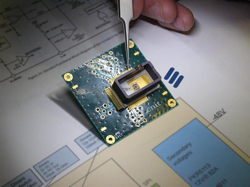 CNIT, Ericsson, Nokia and IMEC demonstrated a packaged graphene-based modulator at MWC 2017
Integration with existing CMOS electronics processes will be critical if graphene is to provide the performance which researchers anticipate. “Graphene-silicon integration is one of the major efforts of the Flagship,” Prof Ferrari explained, “and it’s an issue for a couple of reasons.
“We can’t work on the basis that graphene devices will need to be built on dedicated fabs, which might cost billions of dollars. So, one of the issues is to integrate graphene into CMOS – and it’s one which we’re getting closer to solving.”
The other issue is to enable the creation of silicon photonics. “This is a developing field which has the potential to overcome a number of problems – copper interconnects, for example. But silicon has a few issues when it comes to detecting light. At the moment, that is solved through the use of germanium, but that needs more complex deposition processes.
“However, if you can integrate graphene, you can modulate light on a passive platform. The real vision is to perform detection and modulation in graphene, with processing performed in silicon.”
But there is still a long way to go before graphene is found in mainstream optoelectronics and photonic devices. “We need to make sure we can have coverage at the wafer scale,” Prof Ferrari said, “so we get the same properties as at the small scale. While graphene based devices are easy to make when small, it’s challenging to do it over large areas.
“We also need to make sure graphene retains its properties when integrated into CMOS devices. There is a massive development effort, which has mostly solved the issues at the lab scale, but we need more effort to move graphene to large scale.”
But graphene isn’t the only material that show promise for optoelectronics and photonics. A number of so called 2D materials are also attracting the attention of researchers. “I prefer to call them layered materials,” Prof Ferrari explained. “For example, MoS2 comprises three atomic layers.”
He said many of these layered materials have properties which complement those of graphene. “Band gap, for example. So they are promising for electronics; you could build an IC featuring MoS2, but it would only operate at a frequency specific to MoS2.
“This could enable hybrid devices to be developed. For example, MoS2 would bring responsiveness, while boron nitride would enhance mobility. But, from industry’s point of view, the less hybridisation the better. We need to remember that, while hybrids are potentially good, their manufacture will be more complex.”
Meanwhile, Graphene Flagship researchers from the Institute of Photonic Sciences in Barcelona have shown that it is possible to integrate graphene into a CMOS IC.
The team then created a high resolution image sensor by combining this graphene-CMOS device with quantum dots to create an array of photodetectors. When used as a digital camera, the device can sense UV, visible and infrared light at the same time. Graphene’s high charge mobility enables the device to have high sensitivity.
By using a layering and patterning approach to create a hybrid graphene and quantum dot system on a CMOS wafer, the Flagship team said it solved a complex problem with a simple solution.
First, graphene is deposited, then patterned to define the pixel shape. After this, a layer of PbS colloidal quantum dots is added. Light is absorbed by the quantum dot layer, which transfers it as photo-generated holes or electrons to the graphene, where a bias voltage applied between two pixel contacts causes them to circulate. The photo signal is sensed by the change in graphene’s conductivity.
Prof Ferrari described the work as a key first step. “The Flagship has put a significant investment in the system level integration of graphene and this will increase as we move along the technology and innovation roadmap.”
Meanwhile, the Flagship has just approved a project to integrate graphene into 5G technology. “We want to develop a transceiver that can work at 300Gbit/s,” Prof Ferrari concluded.


