The tasks of the hardware designer
Looking at the tasks of the hardware designer, as summarised in Figure 1, we can examine how each step plays out in reality:
• Technical requirements are specified by management and marketing sources and are often contradictory.
• Understand the requirements and clarify as required.
• Consider multiple options to implement the hardware with the goal of finding one viable option that will meet the requirements, and turn it into an engineering spec.
• Prototype the best options to ensure their viability. Today’s schedules don’t allow for that, so step 4 is no longer part of the process.
• Select the best one, then implement it.
Skipping step 4 means going straight from whiteboard analysis to an implementation, and thus the digital IC designer goes straight to their favourite editor. Months and thousands of lines of code later, and all being well, the designer’s intention is implemented via a mountain of Verilog ‘always’ blocks and is then verified by another team. Ideally, there will be no issues because the pile of RTL code is difficult to change.
But there will always be change; at some point during the implementation phase, it is more than likely the designer will be notified of a ‘small’ change to the requirements.
By the time the project is finished, the next one will always be delayed. Fortunately, the two projects are usually similar, except for some new functionality and different performance targets. However, even a small change necessitates a complete reimplementation, so the designer has to open up the editor again and start over.
A better way
There is good news. Most leading semiconductor companies are moving to a hardware design paradigm that puts more focus on the real design engineering work.
Their hardware engineers create designs at a higher level of abstraction, using languages such as SystemC, C++ and Matlab, then use an automated high-level synthesis tool to translate or – more correctly – synthesise this to RTL for implementation on an ASIC or FPGA. The RTL can be pushed through the rest of the IC tool chain automatically.
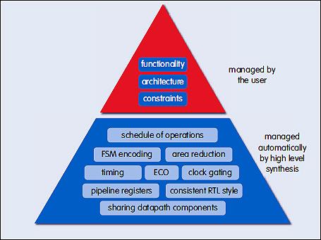
As illustrated in Figure 2, this allows the designer to focus on functionality and high-level architecture in the high-level design. From that design, the HLS tool creates one or more RTL implementations optimised towards the constraints specified by the designer.

Figure 2: Designers can focus on functionality, architecture and constraints, while leaving other factors to the high level synthesis tool
What design improvements can we expect?
So let’s revisit the five design tasks again, from the point of view of a designer who is using high-level synthesis (HLS).
• Getting technical requirements from management or marketing
This is likely to be unchanged and there will still be some requirements that may conflict. However, what will change is that it will not be necessary to figure out later how to implement a required change in the sea of RTL that has already been written. All that is required is to specify the change, which might just be a change to the constraints, and the HLS tool will work out how to create the RTL.
• Take the time to fully understand the requirements, getting clarifications as required
Again, HLS doesn’t fundamentally change the fact that there will never be sufficient time to fully vet the specification. However, it does provide one major advantage: often, it is possible to use a high-level model, such as SystemC, C++ or Matlab, to work through the requirements, knowing that the work to create that model is, in fact, on the direct path to silicon.
• Consider multiple options to implement the hardware
This is the classical engineering work, which is where HLS can really begin to make hardware design great again. Because the designer is working at a higher level of abstraction, it is possible to generate multiple implementations and to evaluate multiple implementation options quantitatively. For example, in Figure 3, a total of more than 80 implementations were considered in terms of power, performance and area from a single high-level SystemC model. With quantitative analysis in hand, the best option for this specific design target can be selected.

Figure 3: Working at a higher level of abstraction allows designers to evaluate multiple implementation options quantitatively
• Prototype the best options to ensure their viability
Depending on the HLS flow, this one may have come for free with #3. Assuming the HLS flow is tightly integrated with the silicon implementation flow, the option(s) selected previously will be viable in silicon.
• Select the best one, and implement it
After taking the above steps, an implementation may already be committed to hardware and the verification team can begin work. So, instead of writing thousands of lines of RTL code, the designer can now focus on tuning the high-level model, which typically comprises at least an order of magnitude less code. So this phase becomes more about optimisation, again a true engineering task, rather than tedious coding of Verilog RTL.
All of these improvements come from working at a higher level of abstraction, working with design decisions and implementation details. Designing hardware in 2017 is set to become more efficient, more interesting and, above all, more fun.
Author profile
Dave Pursley is a senior principal product manager with Cadence Design Systems.


