
It's something that is growing in importance with the development of devices for applications such as the Internet of Things and wearables. These applications need to accommodate analogue inputs, yet they need to be enabled by low power, low cost silicon. Those companies developing chips – largely SoCs – for these applications are looking to meet the low power and low cost targets by following Moore's Law to smaller process nodes. But analogue and leading edge nodes don't go together easily. What are these companies doing to get what is effectively the 'best of both worlds'?
Rene Kohlmann, senior engineering director with Dialog Semiconductor, said the company had already completed SoC designs at the 55nm node which included analogue functionality. "We have integrated digital, analogue and radio circuitry into one component," he said. "The result is a complete solution, with everything required for a Bluetooth Low Energy based device, including an antenna and a lithium battery connection."
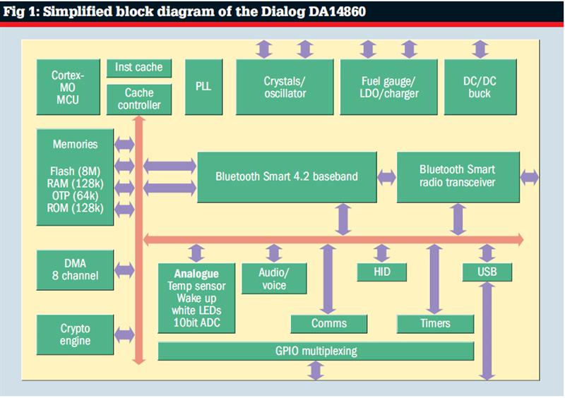
Dialog has recently launched the SmartBond family, which is said to feature the smallest, most power efficient Bluetooth Smart solutions which enable low system cost. So far, five parts have been announced in the range, with the DA14680 the latest to be announced (see fig 1).
"In these SoCs," Kohlmann continued, "the RF and analogue elements are larger than the digital part, so we have to determine how we can get the benefit of moving to advanced nodes."
Another company addressing the need for SoCs for IoT applications is Silicon Labs. Chief technology officer Alessandro Piovaccari highlighted the problem. "Digital scales with process technology, but analogue doesn't scale in the same way. Analogue scaling is driven more by issues such as matching between devices: the two have to be as similar as possible. In the signal chain, matching becomes harder as process technology shrinks."
So how does Silicon Labs address the issue? "What we do is, rather than to rely on matching alone, we look to use the digital domain – it's digitally assisted mixed signal design."
The idea of this, Piovaccari continued, is to handle as much of the processing requirements in the digital domain. "Traditionally, analogue will need things such as big filters. Our approach is to digitise the signal as soon as possible and to applying filtering in the digital domain."
Kohlmann noted that Dialog uses a similar approach. "We are trying to put more capacity into a smaller area. It's not just taking advantage of a process shrink, we can also trade off elements. For example, we can make shift analogue and the radio into the digital domain, but we still need high speed, but low power, A/D and D/A converters. However, there are more parasitics in the analogue domain.
"If you do this, you have to make sure you gain something. If you look at Bluetooth Low Energy, it's all about power and area, so when these SoCs are designed, you have to ensure the circuitry can handle these advantages."
Piovaccari agreed. "The SoCs we are designing for IoT applications will still need pure analogue technology, such as low noise amps and power amps.
"When you start to scale analogue circuitry, you find you get better switches at smaller process nodes and that's how you take advantage – by using those better switches to design different types of analogue circuitry."
One of those different types of analogue circuit to which both referred is the data converter. Kohlmann pointed out: "You typically need a completely new design for data converters and we have developed high speed A/D and D/A converters in house. For example, we have designed an 8bit A/D converter running at 8MHz which draws just 15µA – equivalent to 2.5pJ per conversion."
Piovaccari picked up on his earlier point regarding switches. "Smaller process nodes enable better switches and you can apply that benefit to analogue circuitry. For example, any A/D converter depends on matching techniques and good op amps. But the trend now is to move to SAR converters, which are based on capacitors and switches. With a little bit of digital calibration, we can design good SAR converters." But he also pointed out there will always be some degree of mixed signal design in any SoC intended for IoT applications. "You can't make a converter without capacitors, so these SoCs can never be purely digital."
Another issue which impacts on analogue as process technology shrinks is operating voltage. Gone are the days when analogue devices ran from a 5V supply. "If you go sub micron," Kohlmann pointed out, "you need to reduce the operating voltage towards 1.2V, with a sleep mode that operates from a 900mV supply. You have to make sure that you can overcome these problems. Typically, that means data converters will need a completely new design, but it's also true for the radio components."
Piovaccari accepted lower voltages are a problem. "Getting 20dBm is hard to do with 1.2V, so you need charge pumps and things like that." But, he contended, lower voltages mean less power is consumed and that is good news when the target device is battery powered. "There has been talk of 50billion IoT devices being installed by 2020. It could be that 20bn of those will be battery powered, so it's very important these devices consume the least power possible."
And it's here that smaller processes can help; leading edge processes have lower leakage. "However, once inside the chip," Piovaccari continued, "you deal with impedances. The upper supply limit is a problem, but there's no reason why you can't use current and push more of the design into the current domain."
Kohlmann agreed. "Power consumption of battery powered devices is a key consideration, particularly for wearables, which may only have one small battery. We want that to last for as long as possible."
Is it about functionality or economics? Usually, the decision about which process node to use comes down to economics. "It's about the economies of scale and the availability of processes," Kohlmann said. "It's always a business case. But CMOS will be the way to go, because it's all about reducing current, size and cost. Our latest devices have been done in standard CMOS and we haven't used any tricks to enable the circuitry. Going to 40nm – even 28nm – can be done."
"A more digital centric mixed signal design approach enables the designer to leverage more advanced process nodes in order to resolve one of the most challenging commercial issues with analogue circuit integration – the ability to integrate analogue to reduce cost while increasing functionality," Piovaccari concluded.


