The paper 'Simulations of Ultralow-Power Nonvolatile Cells for Random-Access Memory', which appeared in the January 2020 edition of Transactions on Electron Devices, shows how individual memory cells can be connected together in arrays to make a RAM. It predicts that such chips would at least match the speed performance of DRAM, but do so 100 times more efficiently, and with the additional advantage of non-volatility.
Manus Hayne, who is leading the research, said: “The work published in this new paper represents a significant advance, providing a clear blueprint for the implementation of ULTRARAM memory.”
The Lancaster team solved the paradox of universal memory by exploiting a quantum mechanical effect called resonant tunnelling that allows a barrier to switch from opaque to transparent by applying a small voltage.
Their work describes sophisticated simulations of this process; and proposes a readout mechanism for the memory cells that should improve the contrast between logical states by many orders of magnitude, allowing cells to be connected in large arrays. It also shows that the sharp transition between opacity and transparency of the resonant tunnelling barrier facilitates a highly compact architecture with a high bit density.
On-going work is targeted at the manufacturability of working memory chips, including fabrication of arrays of devices, development of readout logic, scaling of devices and implementation on silicon.

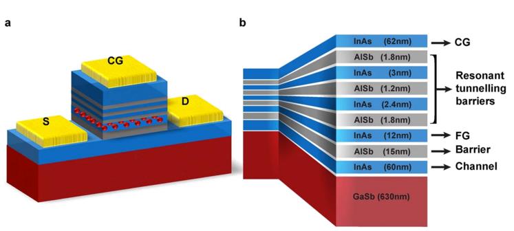
The image above shows the device structure. (a) Schematic of the processed device with control gate (CG), source (S) and drain (D) contacts (gold). The red spheres represent stored charge in the floating gate (FG). (b) Details of the layer structure within the device. In both (a,b) InAs is coloured blue, AlSb grey and GaSb dark red.
Details of the device structure were published by the researchers last year in Nature Scientific Reports. In the paper ‘Room-temperature operation of low-voltage, non-volatile, compound-semiconductor memory cells‘, they explained how "Non-volatile data retention of at least 104 s in combination with switching at ≤2.6 V is achieved by use of the extraordinary 2.1 eV conduction band offsets of InAs/AlSb and a triple-barrier resonant tunnelling structure."


