
The company’s technology uses optical connections and what are known as silicon photonics to move information using light and leading AI chip firms like AMD and Nvidia have begun introducing optical technology into some of their networking chips.
The two new products have been designed to be packaged together with AI chips. One is an interposer, the other a chiplet.
The Passage M1000 is a 3D Photonic Superchip that’s been designed for next-generation XPUs and switches and enables a 114 Tbps total optical bandwidth for more demanding AI infrastructure applications. At more than 4,000 square millimetres, the M1000 reference platform is a multi-reticle active photonic interposer that enables the world’s largest die complexes in a 3D package, providing connectivity to thousands of GPUs in a single domain.
In existing chip designs, interconnects are bandwidth limited because electrical input/output (I/O) connections are restricted to the edges of these chips. The Passage M1000 overcomes this by enabling electro-optical I/O virtually anywhere on its surface for the die complex stacked on top.
This pervasive interposer connectivity is enabled by an extensive and reconfigurable waveguide network that carries high-bandwidth WDM optical signals throughout the M1000. With fully integrated fibre attachment supporting 256 fibres, the M1000 is said to deliver an order of magnitude higher bandwidth in a smaller package size compared to conventional Co-Packaged Optics (CPO) and similar offerings.
The Passage M1000 utilises the GF Fotonix silicon photonics platform which integrates photonic components with high-performance CMOS logic into a single die, creating a production-ready design that can scale effectively with AI demands.
“Passage M1000 is a breakthrough achievement in photonics and semiconductor packaging for AI infrastructure,” said Nick Harris, founder and CEO of Lightmatter. “We are delivering a cutting-edge photonics roadmap that’s years ahead of industry projections. Shoreline is no longer a limitation for I/O. This is all made possible by our close co-engineering with leading foundry and assembly partners and our supply chain ecosystem.”
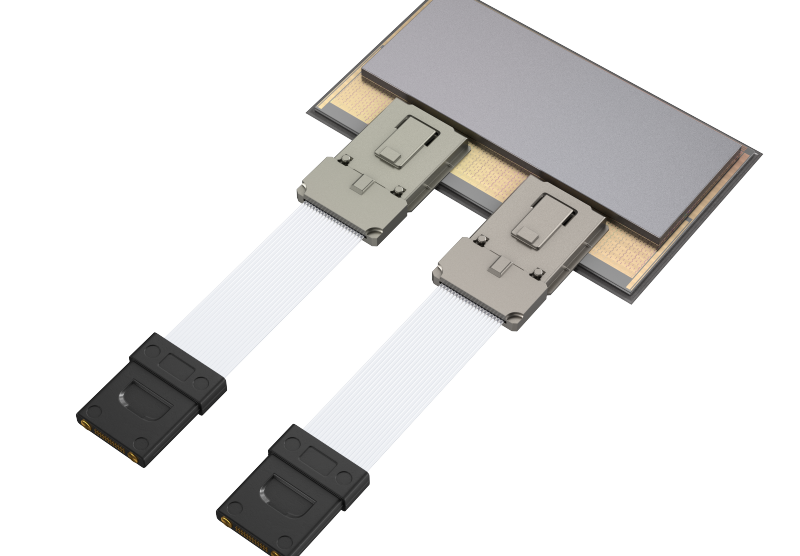
Also announced was Lightmatter’s Passage L200 (above), a 3D co-packaged optics (CPO) product.
The L200 3D CPO family includes both 32 Tbps and 64 Tbps versions, representing a 5 to 10x improvement over existing solutions. This enables over 200 Tbps of total I/O bandwidth per chip package, resulting in up to 8X faster training time for advanced AI models.
The Passage L200 is the world’s first edgeless I/O and can scale bandwidth across the entire die area. This modular 3D CPO solution leverages a standard interoperable UCIe die-to-die (D2D) interface and facilitates scalable chiplet-based architectures enabling integration with next generation XPUs and switches.
The Passage L200 integrates the latest of Alphawave Semi’s chiplet technology portfolio, combining silicon-proven low power and low latency UCIe and optics-ready SerDes with Lightmatter’s photonic integrated circuit (PIC).
Alphawave Semi’s advanced-node electrical integrated circuit (EIC) is 3D integrated on the Passage PIC using standard chip-on-wafer (CoW) techniques. Passage 3D integration enables SerDes I/O to be positioned anywhere on the die, rather than being confined to its shoreline, delivering the equivalent bandwidth of 40 pluggable optical transceivers per L200.
Additionally, multiple L200s can be integrated in a package to serve a broad range of XPU and switch applications.
“AI data centre interconnects face growing bandwidth and power challenges,” explained Andrew Schmitt, founder and directing analyst at Cignal AI. “Co-Packaged Optics (CPO) - integrating optics directly onto XPUs and switches - is the inevitable solution. Lightmatter’s bold approach delivers the essential elements of CPO and gives hyperscalers and chip manufacturers a path to deliver high-performance systems.”
The L200 is engineered for high-volume manufacturing with industry leading silicon photonics fab and OSAT partners including Global Foundries, ASE, and Amkor as well as advanced node CMOS foundries
Lightmatter is offering two product SKUs: the L200 (32Tbps) and L200X (64Tbps) 3D CPO engines building on it Passage technology platform, offering 16 WDM wavelengths per waveguide/fibre with the most advanced and fully integrated photonics control capabilities.
Lightmatter said its interposer will be released in 2025 and the chiplet in 2026.


