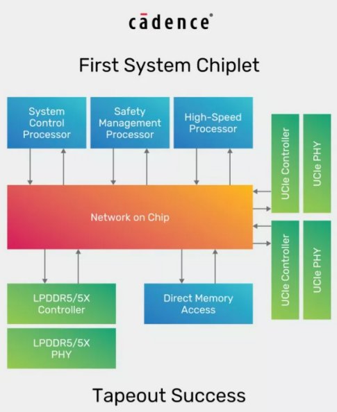
This is being described by the company as a significant leap forward in that it has successfully prototyped, designed, and taped out the industry's first system chiplet – which integrates processors, system IP, and memory IP within a single package, and which is interconnected through the Universal Chiplet Interconnect Express (UCIe) standard interface.
Developed with Arm, the chiplet complies with Arm's Chiplet System Architecture (CSA), a standard that ensures interoperability and speeds time-to-market for chiplets.
A system chiplet includes functionality to manage the resources and functionality of the overall multi-chiplet SoC and features components such as a system processor, safety management processor, Cadence controllers, and Cadence PHY IP for LPDDR5 and UCIe.
Using Cadence Janus NoC technology, the chiplet accommodates up to 64GB/s peak bandwidth for UCIe IP and 32GB/s peak memory bandwidth for LPDDR5 IP.

Earlier this year, Cadence and Arm formalised their longstanding collaboration to deliver a chiplet-based reference design and a cutting-edge software development platform. This partnership combines Cadence's IP and EDA solutions with Arm's state-of-the-art IP technologies, significantly reducing design complexity and accelerating time-to-market for customers.
Further advancements between the two companies are planned, with the aim of offering customers a comprehensive development platform delivering enhanced performance and efficiency.
The central strategy for this collaboration is investing in the Arm CSA, enabling greater component reuse between suppliers. Cadence is an active contributor to the CSA and is developing chiplets that comply with this standard. These standards allow scale and faster time-to-market for chiplets, including Arm Compute Subsystems (CSS) and the Cadence system chiplet.
Abstracting functionality into chiplet IP enables customers to bring innovations to market more quickly.
The shift from monolithic SoCs to chiplet-based designs is driven by the need for enhanced design efficiency, faster platform refresh cycles, and optimised power, performance, and area (PPA) metrics.
Chiplets enable a multi-foundry business model, integrating cross-foundry process technologies within the same package.
As technology density scaling slows, chiplets are becoming essential in overcoming Moore's Law limits and process reticle constraints. New packaging and interconnect solutions, including 2.5D and 3D packaging and die-to-die interfaces like UCIe, support this approach, offering customers a path to accelerated innovation and market readiness.


