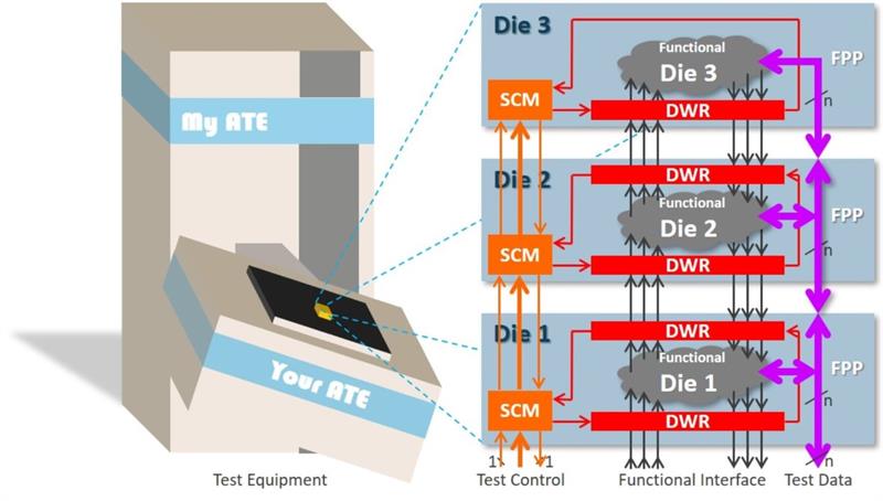
The standard allows die makers to design dies which, if compliant to this standard, constitute, once stacked in a 3D-IC by a stack integrator, a consistent stack-level test access architecture. The standardisation effort of the 3D-DfT (design-for-test) was initiated by imec.
3D-ICs look to exploit the vertical dimension for further integration by stacking dies on top of each other – as a way of keeping the momentum of Moore’s Law going.
According to Eric Beyne, fellow and program director 3D System Integration at imec: “Advances in wafer processing and stack assembly technologies are creating a wealth of different stack architectures. This causes a sharp increase in the number of potential moments at which testing for manufacturing defects can be executed: pre-bond (before stacking), mid-bond (on partial stacks), post-bond (on complete stacks), and final test (on packaged 3D-ICs).
"Test equipment contacts ICs via its external interface through probe needles or at test socket. In a die stack, that external interface typically resides in the bottom die of the stack. For the test equipment to be able to deliver test stimuli to and receive responses from the various dies up in the stack, collaboration from the underlying dies is required to provide test access to the die currently being tested.”
An IEEE working group to standardise 3D-DfT was founded in 2011 by Erik Jan Marinissen, scientific director at imec. In recent years, Adam Cron, principal R&D engineer in the Design Group at Synopsys, has been the driving force as the current chair of the Working Group.
Amit Sanghani, vice president of engineering in the Design Group at Synopsys in Mountain View, California, USA stated: “3D-IC is an important technology to deliver the next wave of innovation as the industry scales past 7nm. Currently, die might come from different suppliers with disjointed DfT architectures. We believe standardising 3D-DfT will benefit our customers by helping form a consistent stack-level DfT architecture and speeding time to market.”

The new standard consists of three main elements. (1) DWR, the die wrapper register: scan chains at the boundary of each die in the stack to enable modular testing of the internals of each die and of the interconnects between each pair of adjacent dies. (2) SCM, the serial control mechanism: a single-bit test control mechanism that transports instructions into the stack to control the test modes of the various die wrappers. (3) FPP, the optional flexible parallel port, i.e., a scalable multi-bit test access mechanism to efficiently transport up and down the die stack the large volumes of data typically associated with production test. While DWR and SCM are based on existing DfT standards, the FPP is truly novel to IEEE Std 1838.
From February 2020 onward, the new standard IEEE Std 1838™ will be available via IEEE Xplore to subscribers of IEEE standards as well as for purchase to everybody else.


